- 您现在的位置:买卖IC网 > Sheet目录490 > NTMFS4833NT3G (ON Semiconductor)MOSFET N-CH 30V 16A SO-8FL
�� �
�
�NTMFS4833N�
�Power� MOSFET�
�30� V,� 191� A,� Single� N� ?� Channel,� SO� ?� 8FL�
�Features�
�?� Low� R� DS(on)� to� Minimize� Conduction� Losses�
�?� Low� Capacitance� to� Minimize� Driver� Losses�
�?� Optimized� Gate� Charge� to� Minimize� Switching� Losses�
�?� These� are� Pb� ?� Free� Devices�
�http://onsemi.com�
�Applications�
�?� Refer� to� Application� Note� AND8195/D�
�?� CPU� Power� Delivery�
�?� DC� ?� DC� Converters�
�?� Low� Side� Switching�
�V� (BR)DSS�
�30� V�
�R� DS(ON)� MAX�
�2.0� m� W� @� 10� V�
�3.0� m� W� @� 4.5� V�
�D� (5)�
�I� D� MAX�
�191� A�
�MAXIMUM� RATINGS� (T� J� =� 25� °� C� unless� otherwise� stated)�
�Parameter�
�Symbol�
�Value�
�Unit�
�Drain� ?� to� ?� Source� Voltage�
�Gate� ?� to� ?� Source� Voltage�
�V� DSS�
�V� GS�
�30�
�±� 20�
�V�
�V�
�G� (4)�
�Continuous� Drain�
�Current� R� q� JA�
�(Note� 1)�
�Power� Dissipation�
�R� q� JA� (Note� 1)�
�T� A� =� 25� °� C�
�T� A� =� 85� °� C�
�T� A� =� 25� °� C�
�I� D�
�P� D�
�28�
�20.5�
�2.7�
�A�
�W�
�S� (1,2,3)�
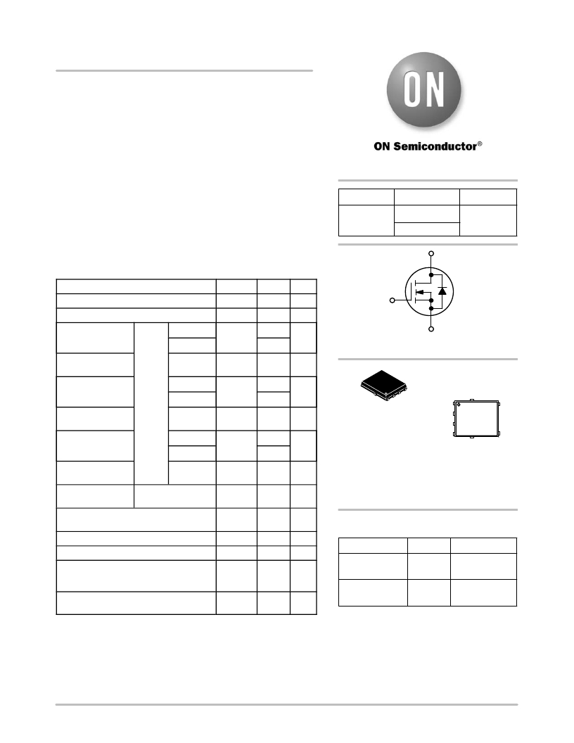
�N� ?� CHANNEL� MOSFET�
�MARKING�
�Continuous� Drain�
�Current� R� q� JA�
�(Note� 2)�
�Power� Dissipation�
�R� q� JA� (Note� 2)�
�Continuous� Drain�
�Current� R� q� JC�
�(Note� 1)�
�Steady�
�State�
�T� A� =� 25� °� C�
�T� A� =� 85� °� C�
�T� A� =� 25� °� C�
�T� C� =� 25� °� C�
�T� C� =� 85� °� C�
�ID�
�P� D�
�I� D�
�16�
�12�
�1.1�
�191�
�138�
�A�
�W�
�A�
�1�
�SO� ?� 8� FLAT� LEAD�
�CASE� 488AA�
�STYLE� 1�
�S�
�S�
�S�
�G�
�DIAGRAM�
�D�
�4833N�
�AYWZZ�
�D�
�D�
�D�
�Power� Dissipation�
�R� q� JC� (Note� 1)�
�Pulsed� Drain�
�Current�
�T� C� =� 25� °� C�
�T� A� =� 25� °� C,�
�t� p� =� 10� m� s�
�P� D�
�I� DM�
�113.6�
�288�
�W�
�A�
�A�
�Y�
�W�
�ZZ�
�=� Assembly� Location�
�=� Year�
�=� Work� Week�
�=� Lot� Traceability�
�Operating� Junction� and� Storage�
�Temperature�
�Source� Current� (Body� Diode)�
�Drain� to� Source� dV/dt�
�T� J� ,� T� STG�
�I� S�
�dV/dt�
�?� 55� to�
�+150�
�104�
�6�
�°� C�
�A�
�V/ns�
�ORDERING� INFORMATION�
�Device� Package� Shipping� ?�
�Single� Pulse� Drain� ?� to� ?� Source� Avalanche�
�Energy� (T� J� =� 25� °� C,� V� DD� =� 30� V,� V� GS� =� 10� V,�
�I� L� =� 35� A� pk� ,� L� =� 1.0� mH,� R� G� =� 25� W)�
�EAS�
�612.5�
�mJ�
�NTMFS4833NT1G�
�NTMFS4833NT3G�
�SO� ?� 8FL�
�(Pb� ?� Free)�
�SO� ?� 8FL�
�1500/Tape� &� Reel�
�5000/Tape� &� Reel�
�Lead� Temperature� for� Soldering� Purposes� T� L� 260� °� C�
�(1/8� ″� from� case� for� 10� s)�
�Stresses� exceeding� those� listed� in� the� Maximum� Ratings� table� may� damage� the�
�device.� If� any� of� these� limits� are� exceeded,� device� functionality� should� not� be�
�assumed,� damage� may� occur� and� reliability� may� be� affected.�
�1.� Surface� ?� mounted� on� FR4� board� using� 1� sq� ?� in� pad,� 1� oz� Cu.�
�2.� Surface� ?� mounted� on� FR4� board� using� the� minimum� recommended� pad� size.�
�(Cu� area� =� 50� mm� 2� [1� oz])�
�(Pb� ?� Free)�
�?For� information� on� tape� and� reel� specifications,�
�including� part� orientation� and� tape� sizes,� please�
�refer� to� our� Tape� and� Reel� Packaging� Specification�
�Brochure,� BRD8011/D.�
�?� Semiconductor� Components� Industries,� LLC,� 2014�
�March,� 2014� ?� Rev.� 10�
�1�
�Publication� Order� Number:�
�NTMFS4833N/D�
�发布紧急采购,3分钟左右您将得到回复。
相关PDF资料
NTMFS4834NT3G
MOSFET N-CH 30V 13A SO-8FL
NTMFS4836NT1G
MOSFET N-CH 30V 11A SO8 FL
NTMFS4837NT1G
MOSFET N-CH 30V 10A SO8 FL
NTMFS4839NT3G
MOSFET N-CH 30V 9.5A SO-8FL
NTMFS4841NT3G
MOSFET N-CH 30V 8.3A SO-8FL
NTMFS4845NT3G
MOSFET N-CH 30V 13.7A SO-8FL
NTMFS4846NT3G
MOSFET N-CH 30V 12.7A SO-8FL
NTMFS4847NAT3G
MOSFET N-CH 30V 11.5A SO-8FL
相关代理商/技术参数
NTMFS4834N
制造商:ONSEMI 制造商全称:ON Semiconductor 功能描述:Power MOSFET 30 V, 130 A, Single N−Channel, SO−8FL
NTMFS4834NT1G
功能描述:MOSFET NFET 30V 130A 3MOHM RoHS:否 制造商:STMicroelectronics 晶体管极性:N-Channel 汲极/源极击穿电压:650 V 闸/源击穿电压:25 V 漏极连续电流:130 A 电阻汲极/源极 RDS(导通):0.014 Ohms 配置:Single 最大工作温度: 安装风格:Through Hole 封装 / 箱体:Max247 封装:Tube
NTMFS4834NT3G
功能描述:MOSFET NFET 30V 130A 3MOHM RoHS:否 制造商:STMicroelectronics 晶体管极性:N-Channel 汲极/源极击穿电压:650 V 闸/源击穿电压:25 V 漏极连续电流:130 A 电阻汲极/源极 RDS(导通):0.014 Ohms 配置:Single 最大工作温度: 安装风格:Through Hole 封装 / 箱体:Max247 封装:Tube
NTMFS4835N
制造商:ONSEMI 制造商全称:ON Semiconductor 功能描述:Power MOSFET 30 V, 104 A, Single N−Channel, SO−8FL
NTMFS4835NT1G
功能描述:MOSFET NFET SO8FL 30V 104A 3.5mOhm RoHS:否 制造商:STMicroelectronics 晶体管极性:N-Channel 汲极/源极击穿电压:650 V 闸/源击穿电压:25 V 漏极连续电流:130 A 电阻汲极/源极 RDS(导通):0.014 Ohms 配置:Single 最大工作温度: 安装风格:Through Hole 封装 / 箱体:Max247 封装:Tube
NTMFS4835NT3G
功能描述:MOSFET NFET SO8FL 30V 104A 3.5mOhm RoHS:否 制造商:STMicroelectronics 晶体管极性:N-Channel 汲极/源极击穿电压:650 V 闸/源击穿电压:25 V 漏极连续电流:130 A 电阻汲极/源极 RDS(导通):0.014 Ohms 配置:Single 最大工作温度: 安装风格:Through Hole 封装 / 箱体:Max247 封装:Tube
NTMFS4836N
制造商:ONSEMI 制造商全称:ON Semiconductor 功能描述:+12 V Telecom Power Conversion Solutions
NTMFS4836NT1G
功能描述:MOSFET NFET 30V 90A 4MOHM RoHS:否 制造商:STMicroelectronics 晶体管极性:N-Channel 汲极/源极击穿电压:650 V 闸/源击穿电压:25 V 漏极连续电流:130 A 电阻汲极/源极 RDS(导通):0.014 Ohms 配置:Single 最大工作温度: 安装风格:Through Hole 封装 / 箱体:Max247 封装:Tube